

Main Menu
E-mail:sales@scmcpcb.com
Website :www.scmcpcb.com
Skype:sc.mcpcb
No minimum order quantity
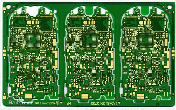
The substrate, or base material, of a PCB is typically fiberglass. The fiberglass that has historically been used for this purpose is designated as FR-4, a flame resistant, woven fiberglass. The next layer is a thin copper foil which is laminated to the board using heat and an adhesive. On top of the copper foil is a soldermask layer. The purpose of the soldermask layer is to insulate the copper to ensure no other metals come into contact with it. The final layer is silkscreen. This is the layer that will add the letters, numbers, and symbols that are commonly seen on PCBs.
Printed circuits are really etched circuits. These circuits can have very few layers or several layers. A copper foil is placed over the fiberglass or a plastic base of each of the layers and is covered with photoresist, a material that loses its resistance or susceptibility to an attack by an etchant or a solvent when exposed to light. When light is sent through the negative image of the circuit paths and onto the photoresist, the areas that remains following the etching are hardened. Any unhardened areas are washed away by an acid bath. To complete the process, the finished layers are glued together.